Influencing RF PCB Thermal Management
With rapid technological innovations in electronics, there is a growing need for special thermal management solutions, especially when it comes to RF circuit boards. Jeffrey Beauchamp, Technical Manager at NCAB Group USA and Mario Cianfriglia, Field Application Engineer at NCAB Group Italy, describe 7 factors influencing RF PCB thermal management.
RF circuit boards operate at high frequencies and require precise alignment of components to reduce signal reflections, noise, and EMI. This requires a specific impedance match that is different from the general circuit board characteristic impedance. It involves matching the impedance at the load and source of the RF signals. A well-matched impedance minimizes loss and enhances performance.
One of the main issues with high-frequency PCBs is that the materials they use to create the layers and conductors heat up as they carry high-frequency signals over long distances. The temperature of these materials increases as the frequency of the signal passes through them, causing energy to dissipate as heat and distort the waveform. This is why it’s important to select a high-quality material for rf circuit board. Ideally, this should be a specialty material that is designed for RF applications and can handle the high-frequency signals without heating up.
The material’s dielectric constant and losses also need to be taken into account. A common FR-4 laminate has a much higher dissipation factor than material that is specifically designed for high-frequency applications, such as Rogers laminates. It also has a lower thermal expansion coefficient, meaning it will expand and pull on copper conductors during repeated thermal cycles, which can cause delamination in extreme cases.
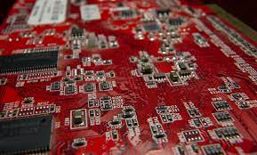
7 Factors Influencing RF PCB Thermal Management
When designing a PCB, it’s important to take all of these factors into consideration. This includes proper stack-up, which is the arrangement of the dielectric and conductive layers. Ideally, the first layer should contain all of the RF components and traces and the last layer should include the non-RF components and traces. This configuration ensures minimum interference between the RF and non-RF components and allows the signals to travel efficiently from the signal layer to the ground plane, minimizing return paths and crosstalk.
It’s also critical to properly size the RF components and traces. This includes reducing the signal wire length and routing them away from other high-speed digital traces, power planes, and any other sources of heat. Additionally, it’s important to use wide copper traces and polygon fills when possible. This will help increase the surface area of the conductors and enable them to dissipate more heat.
Another way to improve RF circuit board thermal management is to use an efficient grounding system. This will reduce the amount of heat that is absorbed by the substrate and will allow it to cool faster. Finally, using thermal interface materials and fans to increase airflow over the circuit board can further improve its ability to dissipate heat.
With the right techniques and knowledge, you can optimize the thermal management of RF circuit boards. By taking these factors into consideration, you can ensure that the high-power RF components in your product work at their optimal temperature and avoid unwanted distortions or signal degradation.